|
|
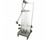
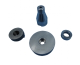
这是我上次做的一个LED球泡灯的UL目击测试温点。
% t4 l4 P4 ~ ILamp base center, inside(represent for lamp base enclosure temperature)
0 K& F7 [% @7 B: {6 d$ RLamp base holder, near to transformer : e2 F8 ]1 \5 r; E* P: p0 U
T1 7 i2 C v+ _( \5 `
Insulation sheet, at bottom side of heat sink, near the bottom of LED package
% s) m: V. t/ P" a2 g6 C* O% wTop Cover, near the heat sink' z m! g3 m' C ?( F- `/ w
Glue of the between the Top Cover and Front Ring Cover ( O5 n0 [7 Z! w- _8 l6 h
Heat Sink, outside, contact surface0 H& v7 q+ ]1 H. w& S
Potting Compound$ H6 r4 _* Q' T1 H8 y0 Y" v) a- L
LED driver :
' M( n0 C4 m' XBobbin of Transformer (T1)0 h' H* e& W5 ?, t
Coil of Transformer (T1)
; Q' R1 Y; ]4 KMulti-layer insulated wire
' [. A, v2 S+ B& _; l! qCoil of Inductor (L1). f( [2 J3 S2 @' H/ k) r+ M! n
Body of Inductor (L1), near Q1
9 B. R3 Y! X3 f9 M" Y1 ~4 k. rFuse F1
- J' @: G+ b0 `6 w3 AC1 body
0 s; S$ w( f/ r+ a8 c5 t# d& kC2 body, near Q1
( V; S' V) A" r9 w* b. m% cCY1 body
/ L, x7 Z, r: ?+ m# m! i4 DVaristor (MOV)
9 F! K& G5 y+ |" E, x5 e/ ZOutput Lead of LED Driver, near the LED package
+ ~4 F+ d5 d5 b; [% ?PWB, top layer, near T1 0 }, Z5 A8 P" T# N0 f" \$ O( O
PWB, bottom layer, near T1 8 I; a, b6 |3 x
PWB, top layer, near Q1
, x" r- E( s2 x2 l) m2 [+ ~LED board:
1 I* F" L# g+ V- |PWB, near LED package
1 D- W6 B3 [, v4 k, q |
|
 |关于安规|小黑屋|安规QQ群|Archiver|手机版|安规网
( 粤ICP13023453-10 )
|关于安规|小黑屋|安规QQ群|Archiver|手机版|安规网
( 粤ICP13023453-10 )


 窥视卡
窥视卡 雷达卡
雷达卡 发表于 2012-3-30 08:23

 显身卡
显身卡