|
|
Question' z( @) ^/ X( B% A' @: z6 P( D; E6 |
1) In case of components mounted on a printed wiring board (PWB) and placed across Q8 B( M2 v. C; z+ N+ x, K/ _
(bridging) insulating distances on the PWB (e.g. providing basic or even reinforced insulation),. v7 s+ Q$ r3 X2 x3 \, z
how to deal with the different distance requirements for distances on the printed wiring
: r, V$ F% J3 r# k3 \6 |material and for distances on other plastics e.g. the housing material of the component
: O+ g* b- c0 l& k(depending on the applicable material group)?5 U; W* I1 z9 @! \+ n3 y
2) In case of components mounted on a printed wiring board (PWB) and placed across
) K. Q. z) ?& X4 @# u4 _1 q! ~insulating distances on the PWB (e.g. providing basic or even reinforced insulation), how to
6 G* {# I7 L4 s! C- y8 ]2 jdeal with the different distance requirements, if the material group for PWB and for the6 I- C+ l% n' ?8 v! T
components placed on it is not the same (e.g. PWB of material group I and relay base of; i2 |9 D" k9 z h( F0 E1 D; A: H
material group IIIa)?
' @/ z- {4 T, }! v& K7 cDecision; t9 o5 a' l6 @/ l( x
1) The defined reduced values for the required creepage distances relevant to printed wiring# j+ z, _7 ~ C& @6 e" k+ C
material in micro-environment of pollution degrees 1 and 2 may only be applied when there
2 J( V, K* l: ^8 kare no components bridging the investigated insulation. If components are bridging insulating
! n% y& e- A# W% ?, k" Idistances on the PWB, the creepage distance requirements relating to the (component)
( A! L1 A* }( }0 zmaterial representing the worst case has to be applied for the PWB also.
+ ?1 k2 j9 v1 }7 s' c5 Q9 v: K2) In case of different material groups for the PWB and the components, again the requirement
* Z& i1 K! G5 \relating to the material representing the worst case has to be used.1 l5 C) _; [0 z
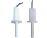
Remark: A component is considered to bridge insulation on the PWB, if the surface of the
9 e/ b0 i8 I6 Y4 t: U I. d2 Ucomponent is located at a distance less than the value “X” (e.g. according to IEC 60664 series)/ ^0 l: J, c/ E& x0 S: i3 E
from the isolating PWB surface. See also enclosed drawing.( Q2 }2 u. q% t- h
, G$ a* r! C) x1 _# d" a
: I1 @: e) _6 |0 S |
|


 窥视卡
窥视卡 雷达卡
雷达卡 发表于 2017-1-7 22:05

 提升卡
提升卡 置顶卡
置顶卡 沉默卡
沉默卡 喧嚣卡
喧嚣卡 变色卡
变色卡 抢沙发
抢沙发 千斤顶
千斤顶 显身卡
显身卡 楼主
楼主